A Unit Under Test (UUT) refers to the specific electronic device or component that is being tested for functionality, performance, and quality. In the context of PCB testing, the UUT typically refers to the printed circuit board (PCB) or any electronic assembly that is undergoing various tests to ensure it meets the required specifications and standards.
At Mirotech, we specialize in providing advanced PCB testing solutions, including custom test fixtures that meet the specific needs of your projects. From bed of nails to linear collapse mechanisms, our test fixtures ensure accurate, reliable, and repeatable results. Whether you’re developing new products or conducting quality assurance, our tailored systems guarantee efficiency and precision.
Why PCB Testing is Essential
PCB testing is a critical part of the electronics manufacturing process, ensuring that your printed circuit boards meet industry standards and perform as expected. Without accurate testing, undetected faults in the unit under test (UUT) could lead to product failures, increased costs, and delays in time-to-market. Mirotech’s testing solutions mitigate these risks by offering comprehensive testing methods designed to fit your specific requirements.
Keypoints to note:
- Detects errors such as opens and shorts
- Verifies circuit logic functionality
- Crucial tool for PCB quality control
At Mirotech, we have over 20 years of experience in the electronics industry, having developed hundreds of test fixtures. Manufacturing such fixtures typically take four to six weeks.
PCB Test Fixtures and Their Uses
Testing Objectives: The goal is to verify the electronic device or component’s functionality, performance, and quality, ensuring it operates correctly and meets design specifications.
Testing Methods: Various methods can be used to test the UUT, including in-circuit testing (ICT), functional testing, and environmental stress testing.
Testing Equipment: Specialized equipment like bed of nails test fixtures, burn-in racks, and custom test rigs are often used.
Data Collection: During testing, data is collected on the UUT’s performance, which is then analyzed to identify any defects or areas of improvement.
Importance: Testing the UUT is crucial for quality assurance in the manufacturing process, helping to ensure that only fully functional and reliable products reach the market.
Typical Bed of Nails Configurations for PCB Testing
Bed of nails fixture designs employ a wide array of spring-loaded pins to contact test points on PCBs, catering to various application needs beyond the basic pogo pin bed. The standard grid array is the most common design, featuring pogo pins arranged in a regular grid of rows and columns, suitable for many boards. For irregularly shaped boards or difficult access points, custom layouts optimize test coverage by matching PCB test pad locations. Clamshell fixtures, with hinged top and bottom pogo pin jig plates, allow access to both sides of the boards by closing over them like a clamping cradle. Flying probe hybrids integrate movable flying probes on x-y axes to reach test nodes that fixed nail positions cannot access. For simpler boards, minimal fixtures or “micro” bed of nails with small matrices of pogo pins reduce setup costs when only a few nodes require validation.
Mirotech manufactures bed of nails test fixtures in the Greater Toronto Area, providing high-quality solutions for efficient and accurate PCB testing.
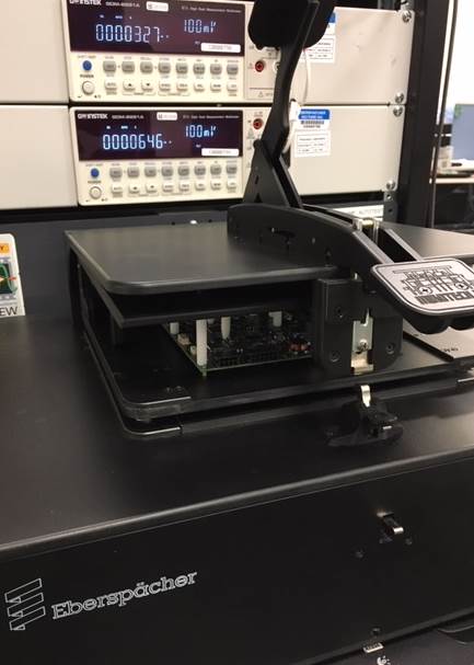
Your UUT is in safe hands, mechanically
The non-wiping mechanism involves a controlled, uniform, and consistent vertical movement during PCB testing. This ensures that all test points on the PCB are contacted simultaneously and with equal force by the test probes or pogo pins. This uniform contact is critical for the following reasons:
Consistent Test Results: By ensuring that each test point receives the same amount of pressure, the non-wiping mechanism contributes to the accuracy and repeatability of test results. This is crucial for identifying faults and verifying the functionality of the UUT.
Minimizing Wear and Tear: A key feature of the non-wiping action is that the test probes make contact with the test points without sliding across them. This reduces wear and tear on both the probes and the PCB, minimizing the risk of damage. As a result, the lifespan of the test fixture and the UUT is extended, reducing the frequency of replacements and repairs.
Enhanced Reliability: The linear collapse design, which incorporates the non-wiping mechanism, ensures precise alignment and reliable connections during testing. This mechanism maintains the integrity of the contact points, contributing to the overall reliability of the testing process.
Protection of Test Components: By avoiding lateral movement or sliding, the non-wiping mechanism protects sensitive components on the PCB. This is particularly important for high-density boards where test points are closely spaced, and any sliding action could cause shorts or other damage.
In summary, the non-wiping mechanism in UUT test fixture design is essential for maintaining the reliability, precision, and efficiency of the testing process. It ensures high-quality results while protecting both the test fixture and the unit under test, ultimately contributing to more robust and reliable electronic products. Whether using a bed of nails or flying probe testing, the principles of controlled, precise contact are critical for achieving accurate and repeatable test results.
Let’s work together on your
next project
We have been providing our customers with test fixtures for over 20 years. We have a proven track record of providing excellent customer service, quality products, and reasonable prices.